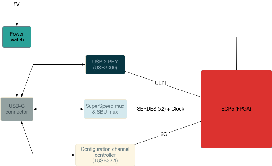
USB-C
The USB-C circuitry on the ECPIX-5 can be used in various configuration. It features the following components:
USB3300 USB 2.0 PHY, capable of acting as USB 2.0 host, device or OTG
HD3SS460 USB-C SuperSpeed+SBU mux for USB 3/PCIe operation
TUSB322I USB-C configuration channel controller
5V power switch for power external devices through the USB-C port
Use cases
ECPIX-5 as a USB 2 peripheral
Thanks to its on-board USB3300 USB 2.0 PHY, ECPIX-5 can be configured as a USB 2.0 peripheral using one the many USB cores available for nMigen (like lambdaUSB or LUNA).
ECPIX-5 as a USB 2 host
In a similar fashion, ECPIX-5 can be configured as a USB 2.0 host for connecting to various USB peripherals such as mice, keyboards or flash drives. There are currently no public nMigen libraries capables of doing so, but you can find some Verilog cores.
By activating ECPIX-5’s power switch, you can provide power to the USB-C connector and power external devices.
ECPIX-5 as a USB 3 peripheral/host
The ECP5 FPGA featured on the ECPIX-5 offers four SERDES, two of which are dedicated to the USB-C connector. Between the USB-C connector and ECP5 there is a mux that can toggle the lines to accodomodate the connector orientation.
USB 3 cores for Migen are currently in a work in progress state.
Non-standard use of the USB-C connector
You can use the USB-C for any application that makes use of SERDES, like PCIe or another SATA port. The USB-C multiplexer is able to route a PCIe clock through the SBU lines.
Pinout
USB 2.0 PHY
PHY pin |
FPGA pin |
Pin description |
|---|---|---|
DATA[0] |
M26 |
ULPI data line |
DATA[1] |
L25 |
ULPI data line |
DATA[2] |
L26 |
ULPI data line |
DATA[3] |
K25 |
ULPI data line |
DATA[4] |
K26 |
ULPI data line |
DATA[5] |
J23 |
ULPI data line |
DATA[6] |
J26 |
ULPI data line |
DATA[7] |
H25 |
ULPI data line |
STP |
H23 |
ULPI stop data stream/last byte of data |
NXT |
F23 |
ULPI next data |
DIR |
F22 |
ULPI data direction |
CLKOUT |
H24 |
ULPI reference clock output |
RESET |
E23 |
USB3300 reset line |
Power switch
Power switch pin |
FPGA pin |
Pin description |
|---|---|---|
EN |
F24 |
High = Power disabled, Low = Power enabled |
SuperSpeed+SBU mux
Mux pin |
FPGA pin |
Pin description |
|---|---|---|
AMSEL |
B26 |
Select configuration (see “ECPIX as USB 3 peripheral/host”) |
POL |
D26 |
Flip polarity (see “ECPIX as USB 3 peripheral/host”) |
EN |
C23 |
Mux enable, active low |
SBU1 |
AF12 (sink) |
100 Mhz reference clock (P), generated by external oscillator |
SBU2 |
AF13 (sink) |
100 Mhz reference clock (N), generated by external oscillator |
LNDP/ LNDN |
AF6/AF 7 |
USB 3 diff pair 1 (RX) |
LNCP/ LNCN |
AD7/AD 8 |
USB 3 diff pair 1 (TX) |
LNBP/ LNBN |
AF9/AF 10 |
USB 3 diff pair 2 (RX) |
LNAP/ LNAN |
AD10/A D11 |
USB 3 diff pair 2 (TX) |
Configuration Channel Controller
Mux pin |
FPGA pin |
Pin description |
|---|---|---|
INT_N |
B24 |
Controller interrupt (active low) |
ID |
D23 |
Device attachment detection (active low) |
DIR |
B23 |
Detected direction: Low=Position 1, High=Position 2 |
SDA |
C24 |
I2C data line (7-bit address: 0x47) |
SCL |
D24 |
I2C clock line |